Electron Microscopy
The George Washington University (GW) Nanofabrication and Imaging Center (GWNIC) features one transmission electron microscope and two scanning electron microscopes.
FEI Teneo LV SEM
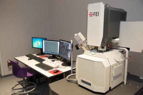
The FEI Teneo LV SEM instrument is a Field Emission Scanning Electron Microscope (FESEM) that combines high and low-voltage ultra-high resolution capabilities with the world’s only low-vacuum, high-resolution imaging solution. Through lens detector for (TLD) SE and BSE detection capable of high-resolution imaging at both high and low kV’s, as well as an Everhart-Thornley SE detector for conventional SE detection. This microscope allows for large area imaging as well as elemental analysis on biological and materials science samples.
- High-resolution FEG column with Schottky source
- 110 x 110 mm, 5-axes motorized (x-y-z-tilt-rotate stage), eucentric stage
- CCD IR inspection camera (NavCam)
FEI Helios FIB SEM
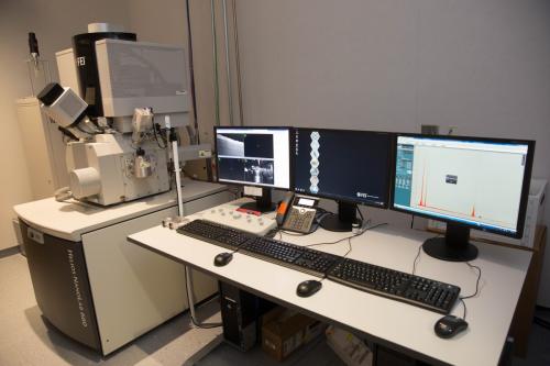
The FEI Helios NanoLab 660 DualBeam is a fully digital, Extreme High Resolution (XHR) Field Emission Scanning Electron Microscope (FE SEM) equipped with Focused Ion Beam (FIB) technology. It allows for fast characterization of nanometer details and analysis in 2D and 3D, high quality thin sample preparation for TEM and flexible nanoprototyping.
The FIB SEM can be used for nanofabrication as well as 3-D reconstruction of biological structures.
-
Schottky field emitter electron source for landing energies 20 V - 30 kV
-
Gallium ion source
-
Everhart-Thornley detector for conventional SE detection
-
Through-the-lens detector (TLD), collecting SE and high-loss BSE, specially designed for high-resolution imaging at both high and low kV's
- The MD mirror detector is designed for excellent contrast of materials at landing energies down to 500 eV
- GIS: W, Pt, insulator deposition and etching
-
EDAX Octane Pro detector for elemental analysis
-
AutoSlice and View G3 MAPS and Correlative Workflow software modules
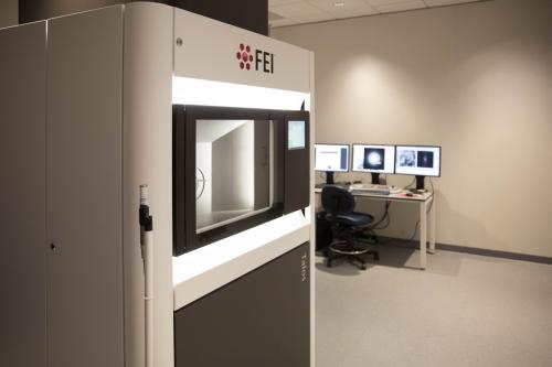
FEI Talos F200X TEM

The FEI Talos™ F200X is a 200 kV FEG Scanning Transmission Electron Microscope (S/TEM), which is designed for fast, precise and quantitative characterization of biological and materials samples. It combines outstanding quality in high resolution STEM and TEM imaging with advances in EDS signal detection and 3D characterization with compositional mapping. In addition, the Talos F200X is equipped with the new Ceta™ 16M camera, which combined with an embedded Piezo-enhanced stage, provides large field-of-view, drift-free imaging with high sensitivity and precise sample navigation. All detectors are silicon solid-state detectors, and can support a beam current up to 3 nA. System Hardware for Talos is STEM Tomography 4.x Data Acquisition Software.
- TEM and STEM imaging modes
- Special applications such as Differential Phase Contrast (DPC)
- X-FEG high-brightness electron source
- Super-X EDS Detector for fast EDS acquisition, mapping and analysis (Silicon Drift Detector (SDD) technology)
- High-Angle, Annular Dark Field detector (HAADF)
- On-axis Bright-Field/Dark-Field STEM detector